

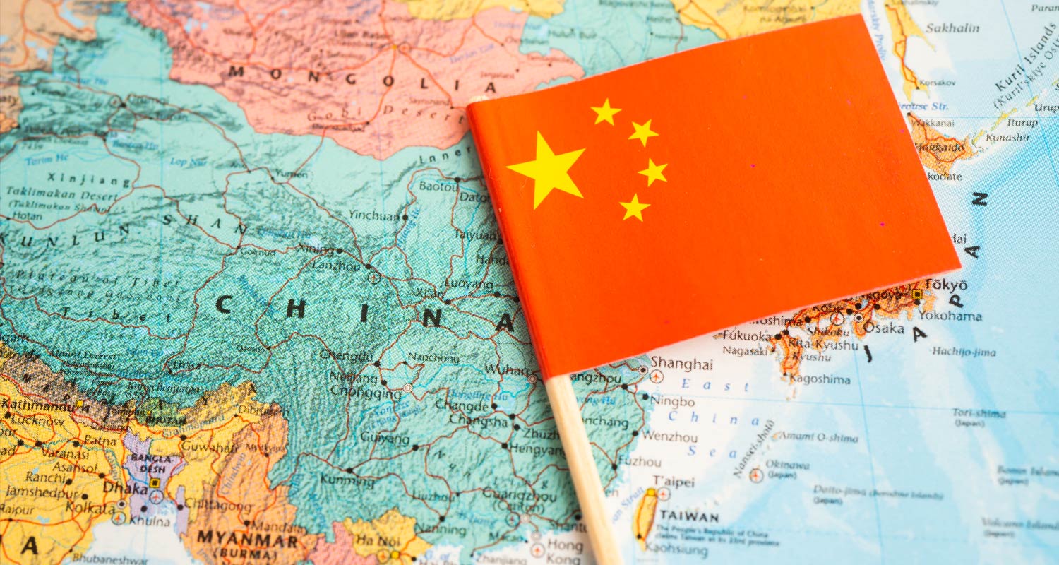
In a high-security Shenzhen laboratory, Chinese scientists have built what Washington has spent years trying to prevent: a prototype of a machine capable of producing the cutting-edge semiconductor chips that power artificial intelligence, smartphones and weapons central to Western military dominance.
Completed in early 2025 and now undergoing testing, the prototype fills nearly an entire factory floor. It was built by a team of former engineers from Dutch semiconductor giant ASML, which reverse-engineered the company’s extreme ultraviolet lithography machines or EUVs, according to two people with knowledge of the project.
EUV machines sit at the heart of a technological Cold War. They use beams of extreme ultraviolet light to etch circuits thousands of times thinner than a human hair onto silicon wafers, currently a capability monopolised by the West. The smaller the circuits, the more powerful the chips.
China’s machine is operational and successfully generating extreme ultraviolet light, but it has not yet produced working chips, the people said.
In April, ASML CEO Christophe Fouquet said that China would need “many, many years” to develop such technology. But the existence of this prototype, reported by Reuters for the first time, suggests China may be years closer to achieving semiconductor independence than analysts anticipated.
Nevertheless, China still faces major technical challenges, particularly in replicating the precision optical systems that Western suppliers produce.
The availability of parts from older ASML machines on secondary markets has allowed China to build a domestic prototype, with the government setting a goal of producing working chips on the prototype by 2028, according to the two people.
Targets
But those close to the project say a more realistic target is 2030, which is still years earlier than the decade that analysts believed it would take China to match the West on chips. Chinese authorities did not respond to requests for comment.
The breakthrough marks the culmination of a six-year government initiative to achieve semiconductor self-sufficiency, one of President Xi Jinping’s highest priorities. While China’s semiconductor goals have been public, the Shenzhen EUV project has been conducted in secret.
Read: Nvidia unveils next-gen AI chips: Vera Rubin and beyond
The project falls under the country’s semiconductor strategy, which state media has identified as being run by Xi confidante Ding Xuexiang, who heads the Communist Party’s Central Science and Technology Commission.
Chinese electronics giant Huawei plays a key role coordinating a web of companies and state research institutes across the country involving thousands of engineers, according to the two people and a third source.
The people described it as China’s version of the Manhattan Project, the US wartime effort to develop the atomic bomb.
“The aim is for China to eventually be able to make advanced chips on machines that are entirely China-made,” one of the people said. “China wants the US 100% kicked out of its supply chains.”
Huawei, the State Council of China, the Chinese embassy in Washington and China’s ministry of industry & IT did not respond to requests for comment.
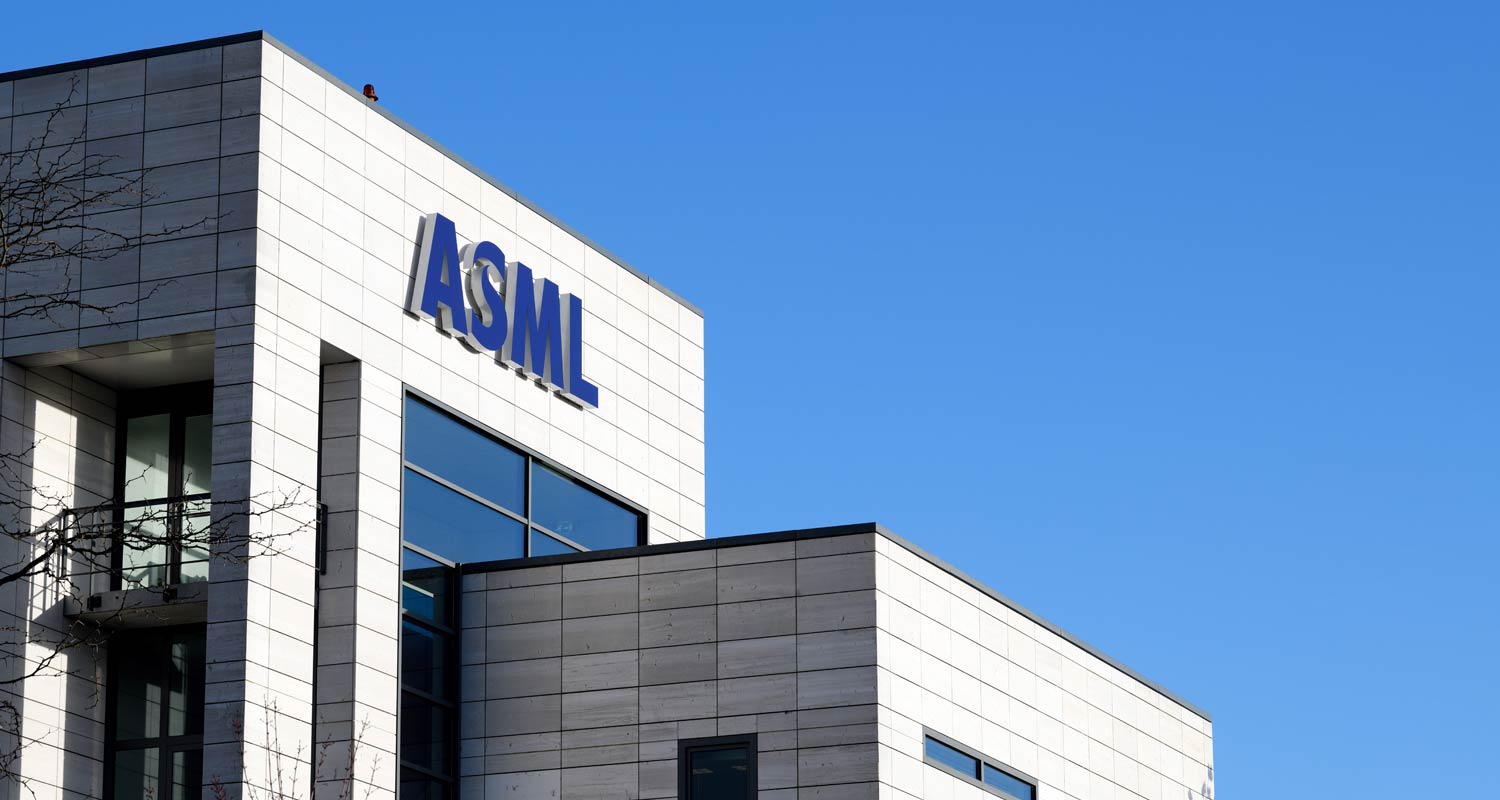
Until now, only one company has mastered EUV technology: ASML, headquartered in Veldhoven in the Netherlands. Its machines, which cost around US$250-million, are indispensable for manufacturing the most advanced chips designed by companies such as Nvidia and AMD – and produced by chip makers such as TSMC, Intel and Samsung.
ASML built its first working prototype of EUV technology in 2001. It took nearly two decades and billions of euros in research and development spending before it produced its first commercially available chips in 2019.
“It makes sense that companies would want to replicate our technology, but doing so is no small feat,” ASML said.
ASML’s EUV systems are currently available to US allies including Taiwan, South Korea and Japan.
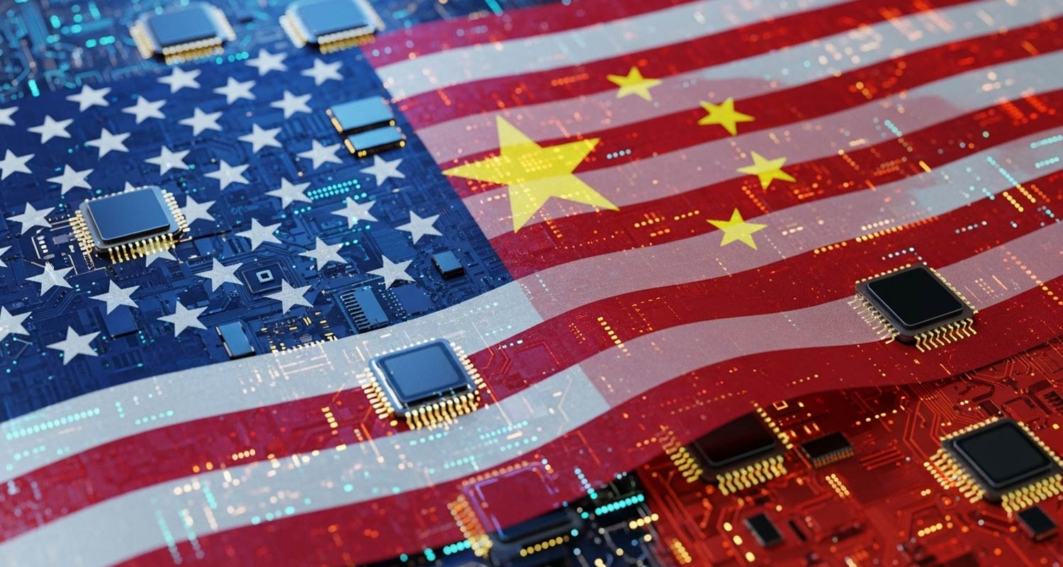
Starting in 2018, the US began pressuring the Netherlands to block ASML from selling EUV systems to China. The restrictions expanded in 2022, when the Biden administration imposed sweeping export controls designed to cut off China’s access to advanced semiconductor technology. No EUV system has ever been sold to a customer in China, ASML said.
The controls targeted not just EUV systems but also older deep ultraviolet (DUV) lithography machines that produce less advanced chips like Huawei’s, aiming to keep China at least a generation behind in chip-making capabilities.
Export restrictions
The US state department said the Trump administration has strengthened enforcement of export controls on advanced semiconductor manufacturing equipment and is working with partners “to close loopholes as technology advances”.
The Dutch ministry of defence said the Netherlands is developing policies requiring “knowledge institutions” to perform personnel screenings to prevent access to sensitive technology “by individuals that have ill intentions or who are at risk of being pressured”.
Export restrictions have slowed China’s progress towards semiconductor self-sufficiency for years and constrained advanced chip production at Huawei, the two people and a third person said. The sources spoke on condition they not be identified due to the confidentiality of the project.
Read: ASML CEO: US restrictions on China ‘economically motivated’
One veteran Chinese engineer from ASML recruited to the project was surprised to find that his generous signing bonus came with an identification card issued under a false name, according to one of the people, who was familiar with his recruitment.
Once inside, he recognised other former ASML colleagues who were also working under aliases and were instructed to use their fake names at work to maintain secrecy, the person said. Another person independently confirmed that recruits were given fake IDs to conceal their identities from other workers inside the secure facility.
The guidance was clear, the two people said: classified under national security, no one outside the compound could know what they were building – or that they were there at all.
The team includes recently retired, Chinese-born former ASML engineers and scientists – prime recruitment targets because they possess sensitive technical knowledge but face fewer professional constraints after leaving the company, the people said.
Two current ASML employees of Chinese nationality in the Netherlands said they have been approached by recruiters from Huawei since at least 2020. Huawei did not respond to requests for comment.
European privacy laws limit ASML’s ability to track former employees. Though employees sign non-disclosure agreements, enforcing them across borders has proven difficult.
ASML won an $845-million judgment in 2019 against a former Chinese engineer accused of stealing trade secrets, but the defendant filed for bankruptcy and continues to operate in Beijing with Chinese government support, according to court documents.
ASML said that it “vigilantly guards” trade secrets and confidential information.
“While ASML cannot control or restrict where former employees work, all employees are bound by the confidentiality clauses in their contracts,” the company said, and it has “successfully pursued legal action in response to the theft of trade secrets”.
Espionage
The company said it safeguards EUV knowledge by ensuring only select employees can access the information even inside the company.
Dutch intelligence warned in an April report that China “used extensive espionage programmes in its attempts to obtain advanced technology and knowledge from Western countries”, including recruiting “Western scientists and employees of high-tech companies”.
The ASML veterans made the breakthrough in Shenzhen possible, the people said. Without their intimate knowledge of the technology, reverse engineering the machines would have been nearly impossible.
Read: China is behind in AI chips – but for how much longer?
Their recruitment was part of an aggressive drive China launched in 2019 for semiconductor experts working abroad, offering signing bonuses that started at C¥3-million to C¥5-million ($420 000 to $700 000) and home-purchase subsidies, according to a Reuters review of government policy documents.
Recruits included Lin Nan, ASML’s former head of light source technology, whose team at the Chinese Academy of Sciences’ Shanghai Institute of Optics has filed eight patents on EUV light sources in 18 months, according to patent filings.
The Shanghai Institute of Optics and Fine Mechanics did not respond to requests for comment. Lin could not be reached for comment.
Two additional people familiar with China’s recruitment efforts said some naturalised citizens of other countries were given Chinese passports and allowed to maintain dual citizenship. China officially prohibits dual citizenship and did not answer questions on issuing passports. Chinese authorities did not respond to requests for comment.
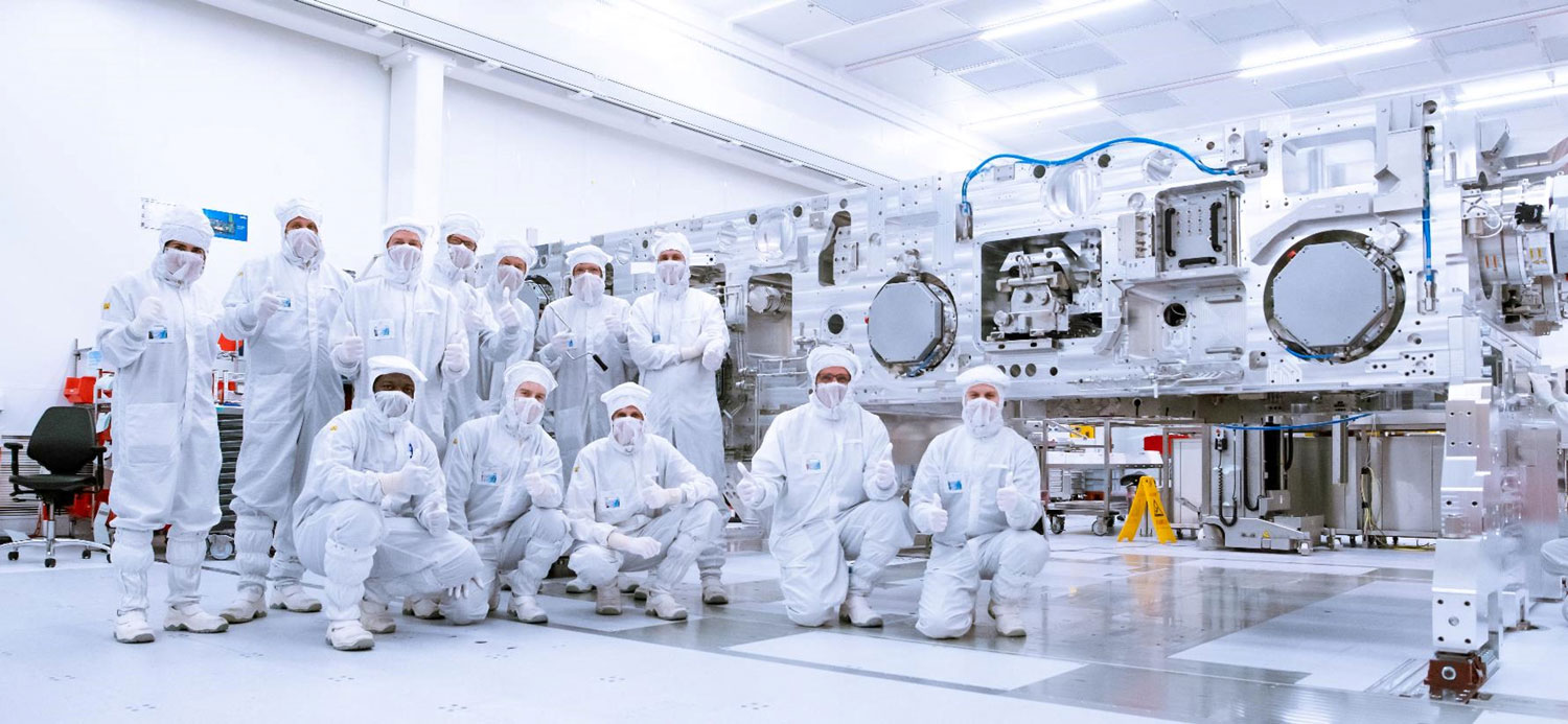
ASML’s most advanced EUV systems are roughly the size of a school bus and weigh 180t. After failed attempts to replicate its size, the prototype inside the Shenzhen lab became many times larger to improve its power, according to the two people.
The Chinese prototype is crude compared to ASML’s machines but operational enough for testing, the people said. It lags behind ASML’s machines, largely because researchers have struggled to obtain optical systems like those from Germany’s Carl Zeiss, one of ASML’s key suppliers, the two people said. Zeiss declined to comment.
The machines fire lasers at molten tin 50 000 times per second, generating plasma at 200 000ºC. The light is focused using mirrors that take months to produce, according to Zeiss’s website.
China’s top research institutes have played key roles in developing homegrown alternatives, according to the two people.
The Changchun Institute of Optics, Fine Mechanics and Physics at the Chinese Academy of Sciences (Ciomp) achieved a breakthrough in integrating extreme ultraviolet light into the prototype’s optical system, allowing it to become operational in early 2025, one of the people said, though the optics still require significant refinement. Ciomp did not respond to requests for comment.
‘Uncapped’ salaries
In a March online recruitment call on its website, the institute said it was offering “uncapped” salaries to PhD lithography researchers and research grants worth up to C¥4-million yuan ($560 000) plus C¥1-million ($140 000) in personal subsidies.
Jeff Koch, an analyst at research firm SemiAnalysis and a former ASML engineer, said China will have achieved “meaningful progress” if the “light source has enough power, is reliable and doesn’t generate too much contamination”.
“No doubt this is technically feasible, it’s just a question of timeline,” he said. “China has the advantage that commercial EUV now exists, so they aren’t starting from zero.”
Read: China will get Nvidia H200 chips – but not without paying Washington first
To get the required parts, China is salvaging components from older ASML machines and sourcing parts from ASML suppliers through second-hand markets, the two people said. Networks of intermediary companies are sometimes used to mask the ultimate buyer, the people said.
Export-restricted components from Japan’s Nikon and Canon are being used for the prototype, one of the people and an additional source said.
Nikon declined to comment. Canon said it was not aware of such reports. The Japanese embassy in Washington did not respond to a request for comment.
International banks regularly auction older semiconductor fabrication equipment, the sources said. Auctions in China sold older ASML lithography equipment as recently as October 2025, according to a review of listings on Alibaba Auction, an Alibaba-owned platform.
A team of around 100 recent university graduates is focused on reverse engineering components from both EUV and DUV lithography machines, according to the people.
Each worker’s desk is filmed by an individual camera to document their efforts to disassemble and reassemble parts – work the people described as key to China’s lithography efforts. Staffers who successfully reassemble a component receive bonuses, the people said.
Huawei’s role
While the EUV project is run by the Chinese government, Huawei is involved in every step of the supply chain from chip design and fabrication equipment to manufacturing and final integration into products like smartphones, according to four people familiar with Huawei’s operations. CEO Ren Zhengfei briefs senior Chinese leaders on progress, according to one of the people.
The US placed Huawei on an “Entity List” in 2019, banning American companies from doing business with it without a licence.
Huawei has deployed employees to offices, fabrication plants and research centres across the country for the effort. Employees assigned to semiconductor teams often sleep on-site and are barred from returning home during the work week, with phone access restricted for teams handling more sensitive tasks, according to the people.
Read: AWS CEO Matt Garman: ‘World will benefit from choice’ in AI chips
Inside Huawei, few employees know the scope of this work. “The teams are kept isolated from each other to protect the confidentiality of the project,” one of the people said. “They don’t know what the other teams work on.” — Fanny Potkin, (c) 2025 Reuters, with additional reporting (c) 2025 NewsCentral Media
Get breaking news from TechCentral on WhatsApp. Sign up here.
